June 29, 2021

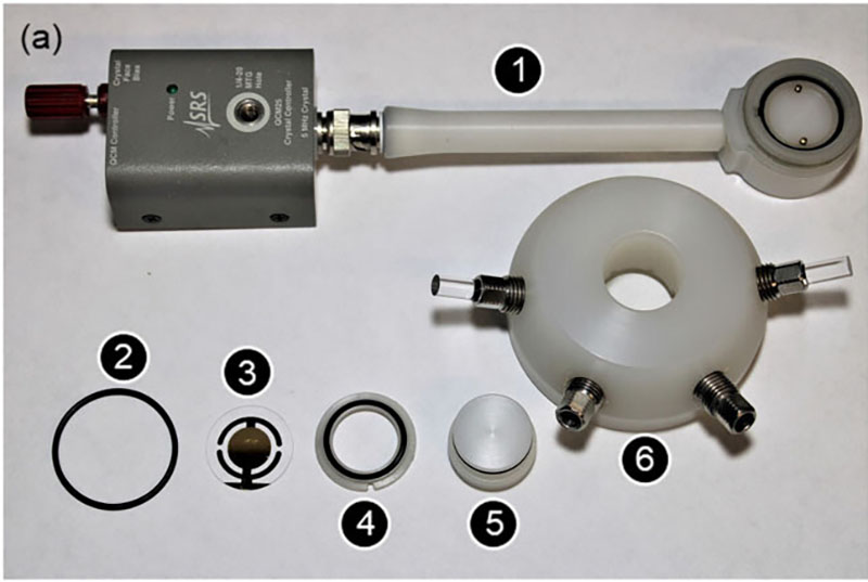
Individual electrode components used to measure mass and thickness of a material during electrochemical operation.
A Mizzou Engineer has designed two techniques for understanding the behavior of materials. In one report, Matthias Young has developed a new way to measure mass and thickness of a material during electrochemical operation. And in a second report, he has developed a technique to measure the atomic structure of disordered materials using microscopic equipment accessible to most researchers. The discoveries could be a game-changer for material scientists working to improve batteries and other technologies.

Young is an assistant professor in the Biomedical, Biological and Chemical Engineering (BBCE) Department and oversees the Mizzou Thin Film Coatings and Materials Electrochemistry Lab.
In a study published in the May 2021 issue of Review of Scientific Instruments, Young modified existing commercial equipment to provide a more efficient process by which to understand what happens as materials charge and discharge. He tested the process using thin films comprised of a well-understood polymer.
Young’s innovation could lead to better batteries, improved water treatment systems and sensing applications such as measuring the amount of nitrate in soil.
“I’m excited to use this new device to help us innovate materials for these applications, and I hope this device will enable the materials science community to accelerate discoveries in other applications,” he said.
Measuring factors simultaneously
In order to develop new materials for applications such as lithium ion batteries, scientists have to understand how materials change dynamically under different charge conditions. It’s a complex process that requires researchers to have insight into what’s happening to materials in real time.
There are existing tools to measure some important factors. Quartz crystal microbalance is an analytical tool that measures mass down to nanograms. Ellipsometry measures thickness and optimal properties based on the way light bounces off a surface and is detected. And electrochemistry tracks behavior as materials are charged or discharged.
“In the past, we had to perform each measurement separately, but we realized we had an opportunity to integrate them and measure them simultaneously,” Young said. “By making some modifications, we were able to bring those three things together. We can measure thickness at the same time as we measure mass changes during electrochemical operation, and better understand what the material is doing while it’s charging and discharging.”
Young plans to make the low-cost device available to other material researchers.
Ryan Gettler, a PhD student in chemical engineering, worked with Young on the project, which had support from the MU Research Council, U.S. Geological Survey and Missouri Water Resource Research center.
An inexpensive way to measure disordered atoms
In a separate study published in the American Chemical Society’s OMEGA, Young outlined a technique to more easily measure the atomic structure of materials using transmission electron microscopes. The process is unique in that it can measure the position of atoms even when they are not in ordered patterns without using a costly facility.
Right now, scientists who want to study disordered atoms in 3D spaces typically rely on the use of a synchrotron, which is a facility about the size of a football field that accelerates electrons to nearly the speed of light to generate X-rays. There are roughly 70 of these billion-dollar facilities in the world, and researchers have to write a proposal and apply in order to access one.
The electron beams used in transmission electron microscopy have previously been problematic for this type of measurement because they interact with and change the composition of materials. In this paper, Young teamed up with cross-campus collaborators to perform the work at cryogenic temperatures of roughly 200 degrees below Celsius.
“What’s cool about it is we can focus an electron beam down to a very small area — a couple hundred nanometers diameter — and measure the atomic structure of a disordered material within that area,” he said.
Knowing the atomic structure of materials at high spatial resolution, as well as understanding the thickness and mass changes during charging and discharging, are critical to understanding and improving materials.
“The properties of a material and how it behaves is dictated by how atoms are arranged in three-dimensional space,” he said. “Atomic structure measurement is the first step toward rationally innovating materials for better performance. But you have to couple atomic structure understanding with a macroscale picture. To interpret materials behavior correctly, you need information on both scales.”
Co-authors of the OMEGA paper were Ahmed Jasim, who has a courtesy appointment in BBCE; Yangchuan Xing, Associate Chair of BBCE; Xiaoqing He, adjunct assistant professor of Mechanical and Aerospace Engineering and senior research specialist at the Electron Microscopy Core; and Tommie White, director of the Electron Microscopy Core at Mizzou. The work was supported through an Excellence in Electron Microscopy award.